|
|
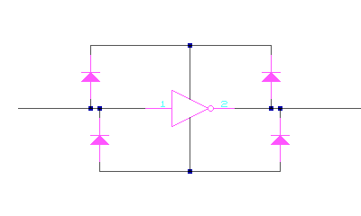
Latch upLatch up is a phenomenon that can destroy integrated circuits. It is well known that most logic devices are equipped with protection diodes. The input pins have added diodes to protect the gates of the input FETs. The output pins tend to have diodes that are an intrinsic part of the output FETs. This means that an over-voltage condition on an input or output will be diverted to the supply pin. If a part is in storage this provides protection against static discharge. Installed in a circuit the situation is more complicated. The protection circuit is supposed to be something like this:
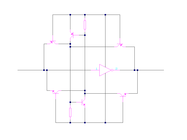
However the protection circuit is probably more like this:
The parasitic thyristor is represented by the middle two transistors in the above diagram. The IC designer will attempt to ensure the base-emitter junctions are shorted out to prevent latch-up, but in practice the impedance at that point is not zero and injecting sufficient current will trigger latch-up. Specialized ICs may be made resistant or immune to latch-up, for example it is possible to create transistors and diodes that are isolated (Silicon-on-insulator) but this adds cost and reduces circuit density. Avoiding latch-upThe simple answer is to avoid the scenario where a pin is driven beyond the supply rail. In a simple logic circuit powered by one supply latch-up should never happen. It becomes a risk when a circuit receives more than one supply and the order of connection cannot be guaranteed. |